[ Instrument Network Instrument R & D ] Recently, the Laser and Infrared Materials Laboratory of the Shanghai Institute of Optics and Fine Mechanics of the Chinese Academy of Sciences has a microstructured photophysics research team led by researchers Zhang Long and Dong Hongxing, and Nanjing Xiaozhuang University, Shanghai Academy of Chinese Academy of Sciences, and other domestic institutions. Research institutes have cooperated to make new progress in the field of microcavity modulated broadband tunable lasers. A new type of wide band-gap tunable CsPbCl3-3xBr3x nanowire-shaped microcavity was realized, and the dynamic characteristics and internal chemical mechanism of ion exchange of the material were analyzed using density functional theory and kinetic experiments. Based on the regular geometry of the microcavity And wideband gap adjustment characteristics, successfully achieve high-quality, wideband tunable micro / nano laser output on a single microcavity.

A nanowire can be defined as a one-dimensional structure that is limited to less than 100 nanometers in the lateral direction (there is no restriction in the longitudinal direction). Suspended nanowires mean that the ends of the nanowires are fixed under vacuum. Typical nanowires have aspect ratios above 1000, so they are often referred to as one-dimensional materials.
Depending on the composition of the material, nanowires can be divided into different types, including metal nanowires, semiconductor nanowires, and insulator nanowires. Nanowires are produced in the laboratory and have not been found in nature as of 2014. Nanowires can be made by suspension, deposition, or elemental synthesis. Suspended nanowires can be obtained by chemically etching thick wires, or they can be produced by bombarding thick wires with high-energy particles (atoms or molecules). There are two types of nanowires grown in the laboratory: nanowires perpendicular to the plane of the substrate and nanowires parallel to the plane of the substrate.
Nanowire micro / nano laser light source with broadband tunable characteristics has important application prospects in micro optoelectronic devices. However, due to the narrow gain range of nanowires, the current research mostly relies on integrating multiple nanowires on a single device to achieve a broadband tunable laser output, which greatly hinders the further miniaturization and integration of optoelectronic devices. In recent years, due to its high absorption coefficient, high fluorescence yield, and large spectral tuning range, perovskite materials have attracted much attention. Many studies have shown that compared with traditional optical materials, perovskite nanowire micro / nano lasers have high quality, low threshold, and broadband tunable characteristics. However, due to the soft lattice characteristics of perovskite materials, it is difficult for a single perovskite nanowire to achieve a broadband tunable laser output. Therefore, new preparation schemes and mechanisms need to be explored to optimize the morphology, crystal quality, and gain range of perovskite nanowires, so as to achieve broadband tunable micro-nano laser output.
In this study, the researchers first prepared high-quality perovskite nanowire-like microcavities through an improved chemical vapor deposition technique, and then successfully achieved wide band-gap tunable fluorescence on a single nanowire based on anionic solid-phase migration reactions. Glow.
Chemical vapor deposition is a chemical technology. The technology is mainly a method of forming a thin film by using a chemical reaction on the surface of a substrate by using one or more gas phase compounds or simple substances containing thin film elements. Chemical vapor deposition is a new technology for preparing inorganic materials developed in recent decades. Chemical vapor deposition has been widely used to purify substances, develop new crystals, and deposit various single crystal, polycrystalline, or glassy inorganic thin film materials. These materials can be oxides, sulfides, nitrides, carbides, or binary or multiple inter-elemental compounds in groups III-V, II-IV, and IV-VI, and their physical functions can be passed through the gas phase. The doping deposition process is precisely controlled. Chemical vapor deposition has become a new field in inorganic synthetic chemistry.
Combining density functional theory, the researchers analyzed the atomic path of anion migration in the perovskite nanostructure, revealed the basic process of ion migration and clarified the source of its ion migration—small ion migration activation energy, which is the material ion migration, The study of phase separation and optical properties has laid a solid theoretical and experimental foundation. Kinetic experiments further support the theoretical results. With the change of reaction time, a single nanowire goes through three main processes: first, the nanowires with uniform luminescence gradually change into adjustable bandgap nanowires; then, the overall nanowire bands The gap is adjustable, but its band gap decreases as the reaction time increases. Finally, the nanowires are assimilated as a whole and converted into a uniformly emitting nanowire, but the overall luminous wavelength is redshifted from the initial stage. The realized nanowire-shaped microcavity has regular geometric structure, smooth surface and broadband tunable characteristics. It can be used as a gain medium and an optical microcavity at the same time, and then a single nanowire broadband tunable laser output is achieved. 480 was successfully obtained experimentally -525 nm broadband tunable micro / nano polychromatic laser.
This study analyzes the atomic path, basic process, dynamic characteristics and chemical mechanism of ion migration in perovskite nanostructures, and uses a single nanowire-shaped microcavity to achieve a broadband tunable laser output for the analysis of perovskite materials. The relationship between ion migration and photoelectric performance provides a solid theoretical and experimental basis, and further advances the research progress of high-quality broadband tunable micro / nano multi-color nano lasers.
Source: Encyclopedia, Shanghai Institute of Optics and Fine Mechanics
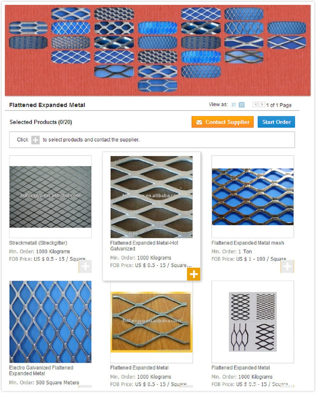
Flattened Expanded Metal
Flattened Expanded Metal
Variety: small, medium and heavy expanded metal mesh. Expanded aluminum mesh, expanded platinum filtration mesh, expanded brass mesh, expanded copper mesh, expanded stainless steel mesh, expanded nickel mesh. Opening in the shape of diamond, hexagonal or special shape.
Use: Used with concrete in buildings and construction, maintenance of equipments, making of arts and crafts, covering screen for first class sound case. Also fencing for super highway, studio, highway. Heavy expanded metal can be used as step mesh of oil tanks, working platform, corridor and walking road for heavy model equipment, boiler, petroleum and mine well, automobile vehicles, big ships. Also serve as reinforcing bar in construction, railway and bridges.
Long way of mesh: TB: 12.5-200mm
Short way of mesh: 5-80mm
Thickness: d: 0.5-8mm
Expanded metal mesh at length from 600-4000mm and width from 600-2000mm


Flattened Expanded Metal,Electro Galvanized Flattened Expanded Metal,Hot Galvanized Expanded Metal,Pvc Coated Expanded Metal
Hebei Fangyu Trade Co., Ltd. , https://www.filtersmaterial.com


