According to reports, South Korea's Ulsan Institute of National Science and Technology (UNIST) recently introduced a new manufacturing method can be called the world's thinnest oxide semiconductor - two-dimensional zinc oxide (ZnO). The semiconductor has only one atomic thickness. This opens up new possibilities for thin, transparent and flexible electronics such as ultra-small sensors.
The new ultra-thin oxide semiconductor was created by a team led by Professor Zonghoon Lee, a professor of materials science and engineering at UNIST.
This material grows a single atom thick layer of ZnO directly on graphene by using atomic layer deposition (ALD). It is also considered a heteroepitaxial layer of the thinnest semiconductor oxide on a single layer of graphene.
Lee said, "Flexible, high-performance equipment is essential for traditional wearable electronics and with this new material we can achieve truly high-performance, flexible devices."
The team noted that performance has become a more critical issue as existing silicon fabrication processes become more elaborate, and much research has been devoted to next-generation semiconductor replacement silicon. Graphene has excellent conductive properties, but it can not be used as a substitute for silicon in electronic products because it has no bandgap. However, in graphene, electrons move randomly at a constant rate, and they do not stop, regardless of their energy.
To solve this problem, the team decided to observe the growth of zinc and oxygen atoms and atoms by observing in situ the preferential zigzag edge of the ZnO monolayer on graphene. Then, they were experimentally determined that the thinnest ZnO monolayer has a wide bandgap (up to 4.0 eV) due to quantum confinement and graphene "super honeycomb" structure, as well as high optical clarity. Existing oxide semiconductors have a relatively large band gap in the range of 2.9-3.5 eV. The larger the band gap energy, the lower the leakage current and excess noise.
The researchers said, "This is the first time that the real observation of the formation of ZnO hexagonal structure in situ through this process, we can understand the two-dimensional ZnO semiconductor production processes and principles."
Lee said, "Heteroepitaxial stacking of the thinnest 2D oxide semiconductor on graphene has the potential for future optoelectronic device applications associated with high optical clarity and flexibility." This study produced a new class of 2D heterostructures , Including semiconductor oxide formed by a high degree of control of the epitaxial growth of the deposition path. "
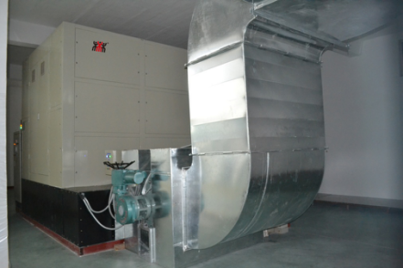
heating storage equipment can provide hot water (<85℃),hot air (<400℃),heat conduction
oil(<300℃) and high temperature steam (100~200℃).
The boiler is widely used in printing drying industry, painting industry , food
processing industry and many other industries heating.
Related Products:hot water supply boiler,steam generating boiler,heat conduction oil furnace.

Industrial Electric Boiler
Industrial Electric Boiler,Energy Saving Industrial Electric Boiler,High Voltage Industrial Electric Boiler,Industrial Hot Air Heater
Dalian Transen Technology Co.,Ltd. , http://www.transen-china.com